Background
One of the major challenges in nanoscale manufacturing is defect control. Optical inspection is not an option at the nanoscale level due to the diffraction limit of light, and without inspection high scrap rates can occur. One solution to this problem is inline metrology using atomic force microscopes (AFM). Single chip MEMS based AFMs have recently been developed that could be easily and rapidly incorporated into fabrication lines. However, metrology with these AFM chips requires accurate placement of specimens relative to the AFM tip.
Technology description
Researchers at The University of Texas at Austin have developed technologies for a mechanical wafer alignment device to enable inline AFM metrology in nano-scale manufacturing by dramatically reducing AFM metrology setup time. The first technology that has been developed is for rapid and repeatable passive alignment of silicon wafers. The method is based on three pins which keep the wafer constrained and a nesting force which keeps the wafer in contact with the pins. The technology consists of a number of features that minimize the probability of wafer jamming and maximizes wafer positioning repeatability. This process has been shown to be capable of positioning repeatability on the order of 1 μm with a setup time of less than thirty seconds. The second technology consists of a positioning stage for an atomic force microscope (AFM) on a chip. The device sits on top of a sample stage via a highly repeatable coupling mechanism. Actuators are used to move the AFM chip to a position of interest on the sample. Flexural bearings couple the actuators to the stage containing the AFM chip. The device allows for translation on the order of millimeters with repeatability on the order of micrometers. The system allows for rapid and precise AFM setup and scanning and supports true inline wafer-scale metrology. Due to its simplicity it can be easily integrated into existing manufacturing processes.
Results
These inventions offer a simple and low-cost technique to achieve rapid wafer alignment with true inline metrology testing in nanotechnology manufacturing. The wing of a Queen Butterfly was chosen for its nanoscale features and representative structure applicable to many hierarchical and photonic materials. Furthermore, the structure of the individual scales is an excellent test case due to the presence of both μm-scale wing “ribs” and nm-scale wing “ligaments.” Additional features may be found in the peer-reviewed journal article.
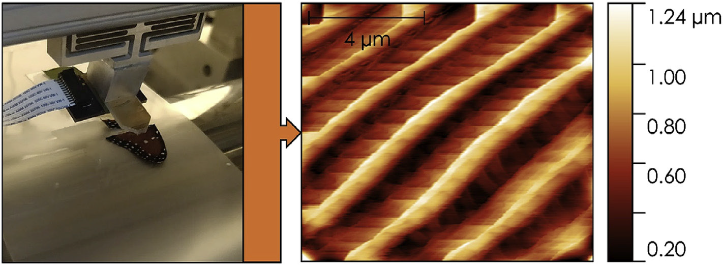
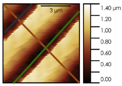
Inline sc-AFM scan of butterfly wing and 33.7s scan of butterfly wing