Background
In the microelectronics industry, nanoscale features are patterned using photolithography, a process in which a transparent mask is used to transfer patterns onto a light-sensitive chemical photoresist on a substrate. The chemical change in the resist enables unwanted material to be etched so that the underlying layer can be patterned. While this method has enabled the mass production of 32 nm node technologies (single patterning), the use of both the resist and transparent mask requires a series of processing steps to ensure proper alignment and resist adhesion.
Typical patterning schemes for metals and metal oxides require multiple processing steps including deposition of the metal, the entire photolithographic cycle, an etch to transfer the resist pattern to the underlying substrate, deposition of the desired material in the adjacent trenches, and finally chemical mechanical polishing. A modern CMOS wafer will go through this photolithographic cycle up to 50 times.
The ability to create nanoscale metal and metal oxide patterns is a requirement of a variety of applications, including microelectronics and carbon nanotubes. Typically, metal patterning processes are performed through a complicated series of lithography and etch steps, which are often wasteful and expensive.
Technology description
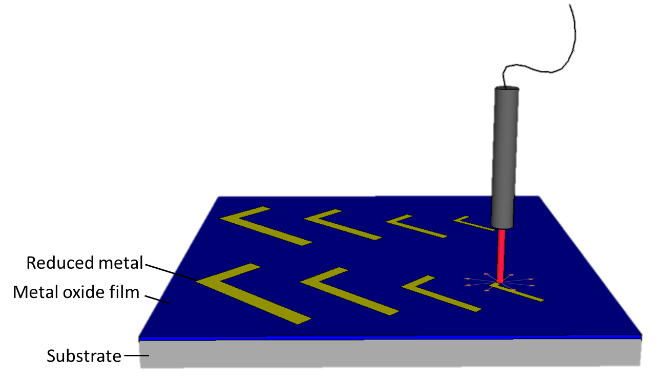
Researchers at The University of Texas at Austin have developed a new process for nanopatterning metals by the local thermally activated reduction of an oxide film with a nanotip. This process of selective reduction is shown capable of producing features with a radius of 10 nm using a tip with a 10 nm radius of curvature, in substantially fewer steps than conventional lithography processes. Ideal process parameters, to optimize writing rate and resolution, are determined using finite element simulations. This technique is especially advantageous for applications where nanoscale writing of 3D conductive materials is desirable, such as magnetic bit memory and nanowires.
Results
A new direct-write patterning method called selective redox takes advantage of temperature control on the nanometer scale to create comparable features. The focus was on selective reduction, but the governing mechanisms are identical for selective oxidation. In selective reduction, a reducing gas such as hydrogen or oxygen flows over the surface of the thin metal oxide film. A thermal probe is used to selectively and locally heat the appropriate regions to a temperature for the reaction to occur. Selective reduction provides a means to write metal nanopatterns precisely.
As it is a direct-writing method, it lends itself to making any desired pattern on a surface, which is valuable for maker spaces and lean manufacturing. It does not require an expensive lithographic mask, reducing cost, and effectively decreases the more than thirteen processing steps required to create nanoscale metal patterns using traditional lithography techniques to one. Moreover, the throughput of this method can be increased by increasing the number of probes employed. More information can be found in the public pending patent application.
Simplified technology schematic