Background
The mid-infrared (mid-IR) wavelength range (~2-20 μm) is of vital importance for a range of sensing, security and defense, and fundamental science applications. Mid-infrared optical sources have historically fallen into two primary categories: simple thermal sources and coherent, laser sources of light. The former consist solely of a hot object, heated to a temperature where the object gives off significant thermal radiation across the mid-IR. Such sources are broadband, covering the entire mid-IR range, but are also slow and extremely power inefficient. Laser sources, on the other hand, can offer high powers and collimated beams, as well as faster modulation. Early mid-IR lasers were typically gas lasers (CO2 and HeNe) offering coherent emission only at distinct wavelengths corresponding to optical transitions in a few gases.
Technology description
Researchers at The University of Texas at Austin have developed growth techniques to grow quantum nanostructures (quantum dots, QDs) of InGaSb in an InAs matrix. These QDs are so-called “type-II” quantum dots, where electrons in the conduction band of the InAs recombine with holes confined in the InGaSb. Because of the additional quantum confinement offered by the QD structures, a significant decrease in Auger recombination is expected. Previous work by the Wasserman group has shown longer lifetimes and improved temperature performance for QD emitters when compared to quantum well (QW) emitters at the same wavelength.
Secondly, the researchers have developed techniques to grow these QD emitters above a layer of highly doped (n++) InAs. This InAs layer is doped to such high levels that it becomes optically metallic in the mid-IR. Leveraging a number of unique effects associated with dipole emitters in the near field of such “plasmonic” layers in order to strongly enhance the radiative lifetimes of the QD emitters.
These devices are the first examples of quantum engineered emitters integrated monolithically with plasmonic materials (in the same material system, and the same epitaxial growth). Devices have been grown and characterized electrically driven plasmonic/quantum engineered emitters with performance better than commercially available mid-IR LEDs operating at the same wavelength.
Results
The proposed structure consists of an n++ epitaxial layer, on the order to 500-1500nm thick, doped to have a plasma wavelength at <7um. Above this a diode structure was grown, consisting of a n-doped InAs layer followed by a p-doped InAs layer, with an unintentionally doped layer between the n and p material which contains some number of QD layers. For additional information on this technology, please see the published paper in Optica.
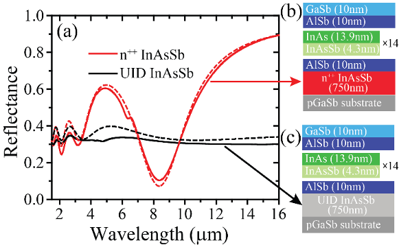 | 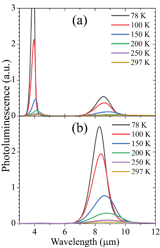 |
Fig. 1: Reflectance vs. wavelength for the devices to the right of the plot. | Fig. 2: Photoluminescence vs. wavelength comparison for the n++ doped device (a) and an undoped device (b). |